Study shows: 2D materials rotate light polarisation
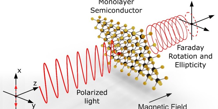
It has been known for centuries that light exhibits wave-like behaviour in certain situations. Some materials are able to rotate the polarisation, i.e. the direction of oscillation, of the light wave when the light passes through the material. This property is utilised in a central component of optical communication networks known as an "optical isolator" or "optical diode". This component allows light to propagate in one direction but blocks all light in the other direction. In a recent study, German and Indian physicists have shown that ultra-thin two-dimensional materials such as tungsten diselenide can rotate the polarisation of visible light by several degrees at certain wavelengths under small magnetic fields suitable for use on chips. The scientists from the University of Münster and the Indian Institute of Science Education and Research (IISER) in Pune, India, have published their findings in the journal Nature Communications.
One of the problems with conventional optical isolators is that they are quite large with sizes ranging between several millimetres and several centimetres. As a result, researchers have not yet been able to create miniaturised integrated optical systems on a chip that are comparable to everyday silicon-based electronic technologies. Current integrated optical chips consist of only a few hundred elements on a chip. By comparison, a computer processor chip contains many billions of switching elements. The work of the German-Indian team is therefore a step forward in the development of miniaturised optical isolators. The 2D materials used by the researchers are only a few atomic layers thick and therefore a hundred thousand times thinner than a human hair.
"In the future, two-dimensional materials could become the core of optical isolators and enable on-chip integration for today's optical and future quantum optical computing and communication technologies," says Prof Rudolf Bratschitsch from the University of Münster. Prof Ashish Arora from IISER adds: "Even the bulky magnets, which are also required for optical isolators, could be replaced by atomically thin 2-D magnets." This would drastically reduce the size of photonic integrated circuits.
The team deciphered the mechanism responsible for the effect they found: Bound electron-hole pairs, so-called excitons, in 2D semiconductors rotate the polarisation of the light very strongly when the ultra-thin material is placed in a small magnetic field. According to Ashish Arora, "conducting such sensitive experiments on two-dimensional materials is not easy because the sample areas are very small." The scientists had to develop a new measuring technique that is around 1,000 times faster than previous methods.
The German Research Foundation (DFG), the Alexander von Humboldt Foundation, the Indian technology foundation I-Hub, the “Science and Engineering Research Board” (SERB) of the Indian Ministry of Technology and the Indian Ministry of Education are jointly financing the project.
Original publication
Carey, B, Wessling, N K, Steeger, P et al. (2024): Giant Faraday rotation in atomically thin semiconductors. Nat Commun 15, 3082. DOI: 10.1038/s41467-024-47294-5
Further literature on the methods
Carey, B, Wessling, N K, Steeger, P et al. (2022): High-Performance Broadband Faraday Rotation Spectroscopy of 2D Materials and Thin Magnetic Films. Small methods; DOI : 10.1002/smtd.202200885
